Bow & Twist Circuit Board Issue and Prevention
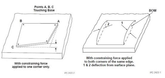
The bow and twist issue on Printed Circuit Board can cause components and parts to shift in the PCB assembly process, if the surface mount and through hole components x/y and z coordinate does not match the pcb, then it will make the PCB assembly process very time consuming and difficult.
IPC-6012 defines the maximum bow and twist 0.75% on circuit boards, however some strict designs only allow bow and twist not to exceed 0.5%. See below for IPC guidelines on how to measure bow and twist.
Prevention of bow and twist on electronic circuit boards:
1. PCB Design: PCB designers should use copper thieving if necessary to balance the design from layer to layer to distribute the copper evenly.
2. Lamination: Prepreg between PCB layers must be symmetrical unless there is specific impedance requirements.
3. Multi-layer pcbs should use the same material manufacturer’s core and prepreg because different manufacturers could cause problems during lamination.
6. Very thin pcb’s can warp and twist very easily so they should be watched during every process.
7. Bake the pcb’s to ensure no moisture and to place on flat surface during cooling.
8. Boards will blind and buried vias are more prone to bow and twist so they must be handled carefully and controlled during the manufacturing process.
Bow and twist issues not only occur in the pcb manufacturing process, but also are caused by uneven copper distribution in the Gerber files.
Circuit board designers should design a multilayer pcb using a symmetrical stack up if no impedance or special requirements are needed. Copper weights should be symmetrical as well as Prepreg and Core thicknesses.
Contact MCL today for help with preventing bow and twist.


